Abstract
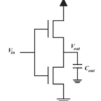
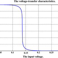
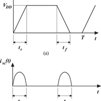
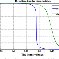
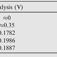
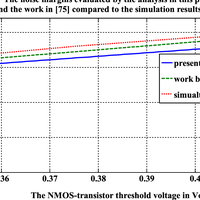
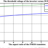
There is no doubt that operating the MOSFET transistor in the subthreshold region, where the power-supply voltage is less than the threshold voltage, has an increasing importance due to the reduced power consumption. In this paper, the analysis of the CMOS logic inverter in the subthreshold region is addressed quantitatively with the static and dynamic characteristics investigated and compared with that operating in the superthreshold region. Specifically, compact-form equations are derived for the output-low voltage, output-high voltage, maximum-input voltage at logic “0,” minimum-input voltage at logic “1,” and threshold voltage of the inverter. Also, the static-power consumption and dynamic-power consumption are investigated and equations are derived for them. Compact-form expressions are derived for the low-to-high and the high-to-low propagation delays along with the fan-out. Qualitative discussions are also provided. The results of the quantitative analysis are verified by comparison with the simulation results adopting the 65 nm CMOS technology.
Figures
![Figure 3 The small-signal equivalent circuit of the subthreshold transistor taking into account the output resistance [53]. It is identical to that of the superthreshold one but the expressions of gm and ro differ.](https://s3-eu-west-1.amazonaws.com/com.mendeley.prod.article-extracted-content/images/c72f108d-1e7b-341c-b00d-601a0ae8dd4d/thumbnail-b54816dd-09b1-4594-9dc5-81a75d208976-2.png)
Author supplied keywords
Register to see more suggestions
Mendeley helps you to discover research relevant for your work.
Cite
CITATION STYLE
Sharroush, S. M. (2018). Analysis of the subthreshold CMOS logic inverter. Ain Shams Engineering Journal, 9(4), 1001–1017. https://doi.org/10.1016/j.asej.2016.05.005
